Nanofabrication
Nanofabrication stands at the forefront of modern physics research, offering a gateway to the manipulation of matter at the atomic and molecular scale. Our research goals require the fabrication of various such nanoscale devices. This provides unique opportunities to engage in cutting-edge fabrication projects that not only contribute to scientific advancement but also provide a hands-on experience in a cleanroom environment. The Quantum Nano Fabrication and Characterization Facility (QNFCF) at the University of Waterloo hosts a state-of-the-art cleanroom, numerous equipment and a dedicated staff for training and maintainance of the facility.

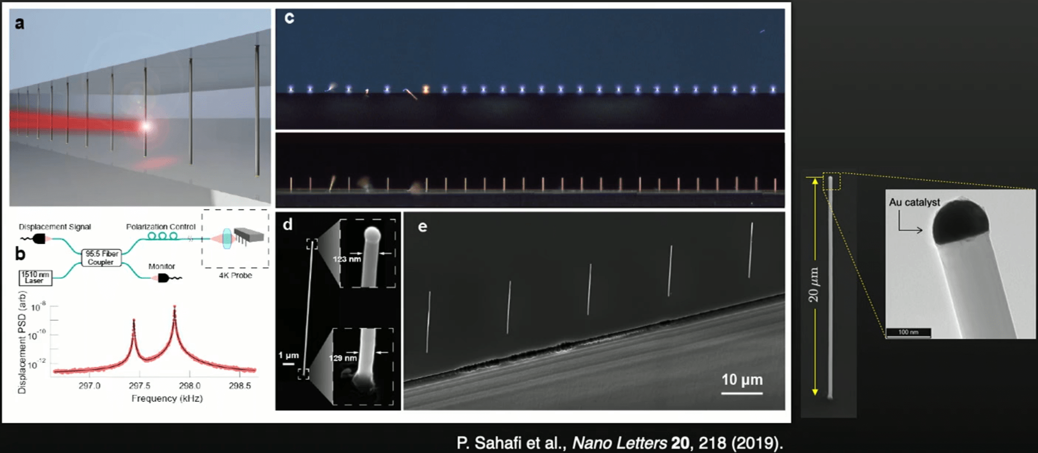
Our experiments utilize ultrasensitive force detectors made from silicon nanowires. These nanowires are grown in-house using QNFCF’s CVD (Chemical Vapor Deposition) system. The growth process involves several crucial and sensitive steps carried out in the cleanroom, which is equipped with state-of-the-art tools including e-beam lithography, UV lithography, e-beam evaporation, and rapid thermal processing.

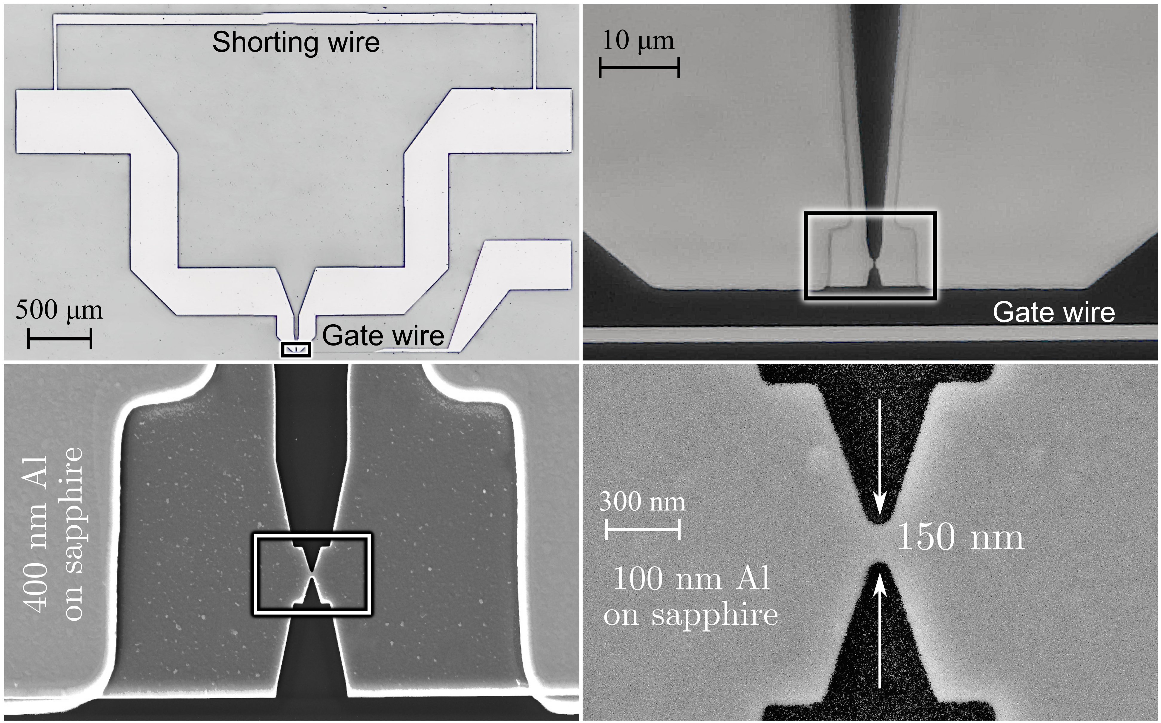
Additionally, we are also engaged in nanofabrication for nanoscale current focusing field gradient devices (CFFGS), which involves steps such as reactive ion etching, e-beam lithography, and plasma-enhanced CVD. Above are some SEM images of the current-generation CFFGS used for our recent work on DNP [1]. The images show zoomed in images of various sections of the device. The image at the bottom right shows the center of the device. The sample is placed above this region so that it experiences the maximum magnetic field gradients generated by the device.

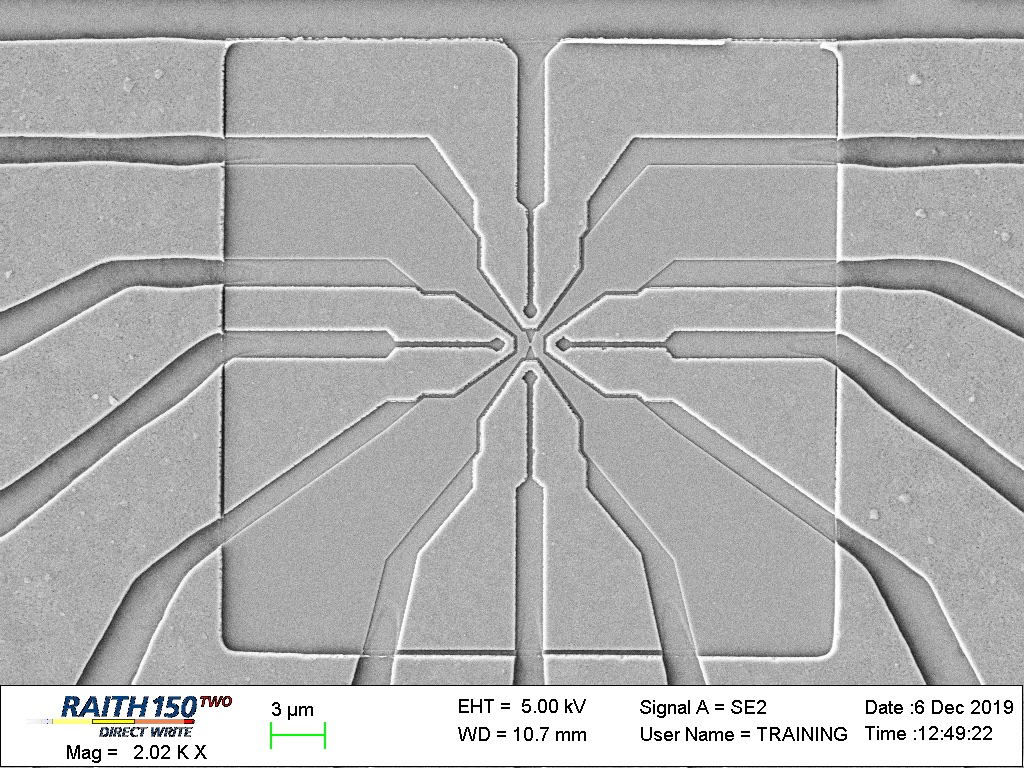
Shown here is an SEM of the new-generation CFFGS that will be used for the upcoming NMRd and spin transport experiments. In the coming days, we have plans to create next-generation CFFGS optimized for operation in the X band. The nanofabrication of these field gradient sources and the growth of ultrasensitive silicon nanowires constitute two critical processes within our work at the QNFCF.

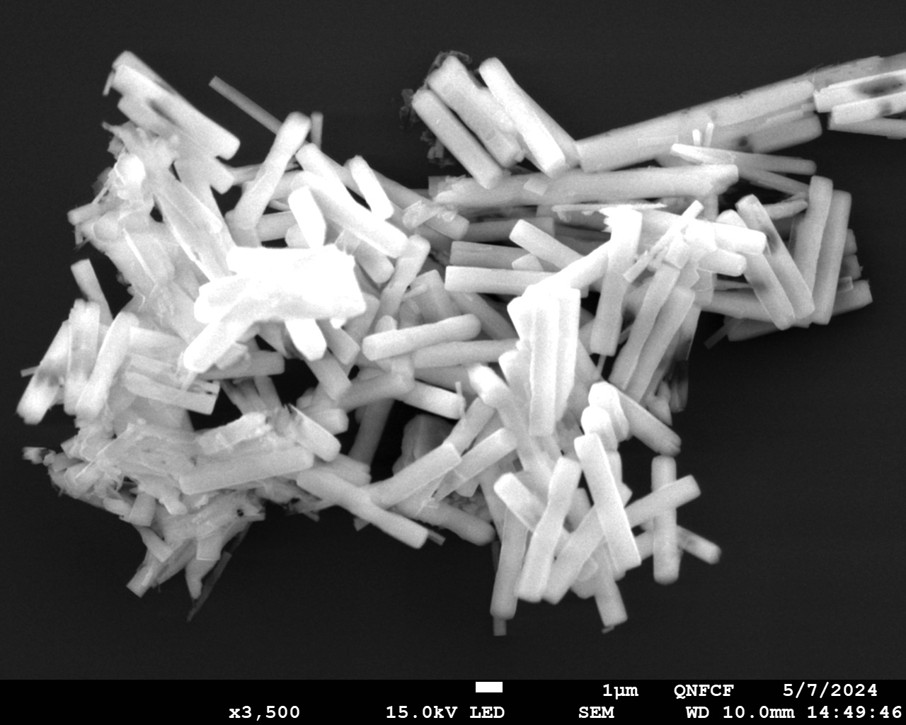
The group often focusses on studying exotic samples. This requires preparing interesting samples and characterizing their properties. Here is an SEM image of recently grown fluorapatite nanorods. These nanorods would be attached to the silicon nanowires which requires developing sample attachment protocols. Once the samples are attahced they are then loaded into the probe for measurements.
Most of the steps involved in these processes are performed in the cleanrooms here at the University of Waterloo. Here are the links for the virtual tours to various cleanroom facilities under QNFCF.